- 您现在的位置:买卖IC网 > Sheet目录3873 > PIC16F627-04/P (Microchip Technology)IC MCU FLASH 1KX14 COMP 18DIP
2003 Microchip Technology Inc.
Preliminary
DS40300C-page 65
PIC16F62X
11.3.2
PWM DUTY CYCLE
The PWM duty cycle is specified by writing to the
CCPR1L register and to the CCP1CON<5:4> bits. Up
to 10-bit resolution is available: the CCPR1L contains
the eight MSbs and the CCP1CON<5:4> contains the
two LSbs. This 10-bit value is represented by
CCPR1L:CCP1CON<5:4>. The following equation is
used to calculate the PWM duty cycle in time:
EQUATION 11-1:
PWM DUTY CYCLE
CCPR1L and CCP1CON<5:4> can be written to at any
time, but the duty cycle value is not latched into
CCPR1H until after a match between PR2 and TMR2
occurs (i.e., the period is complete). In PWM mode,
CCPR1H is a read-only register.
The CCPR1H register and a 2-bit internal latch are
used to double buffer the PWM duty cycle. This double
buffering is essential for glitchless PWM operation.
When the CCPR1H and 2-bit latch match TMR2
concatenated with an internal 2-bit Q clock or 2 bits of
the TMR2 prescaler, the CCP1 pin is cleared.
Maximum PWM resolution (bits) for a given PWM
frequency:
EQUATION 11-2:
MAXIMUM PWM
RESOLUTION
For an example on the PWM period and duty cycle
calculation, see the PICmicro Mid-Range Reference
Manual (DS33023).
11.3.3
SET-UP FOR PWM OPERATION
The following steps should be taken when configuring
the CCP module for PWM operation:
1.
Set the PWM period by writing to the PR2
register.
2.
Set the PWM duty cycle by writing to the
CCPR1L register and CCP1CON<5:4> bits.
3.
Make the CCP1 pin an output by clearing the
TRISB<3> bit.
4.
Set the TMR2 prescale value and enable Timer2
by writing to T2CON.
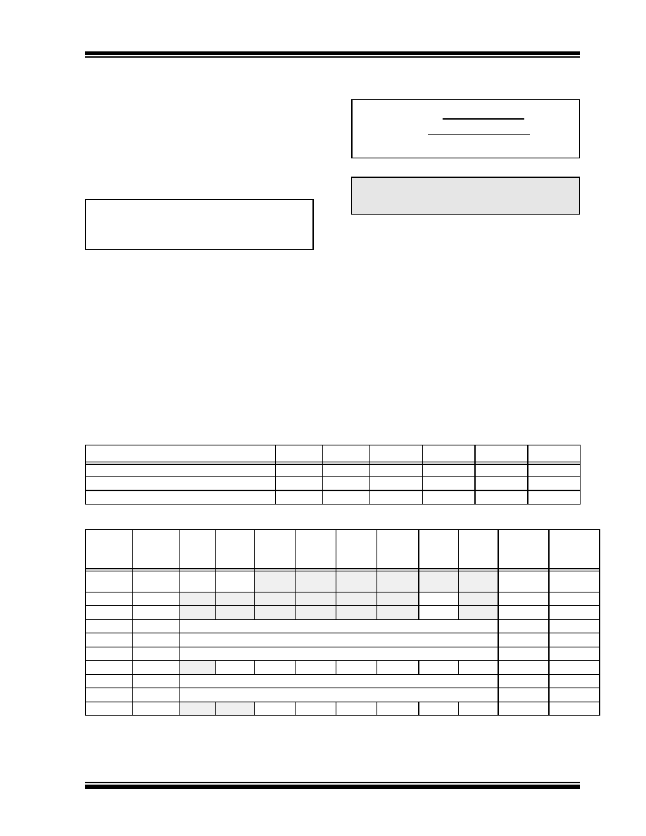
TABLE 11-4:
EXAMPLE PWM FREQUENCIES AND RESOLUTIONS AT 20 MHz
TABLE 11-5:
REGISTERS ASSOCIATED WITH PWM AND TIMER2
PWM duty cycle = (CCPR1L:CCP1CON<5:4>)
Tosc
(TMR2 prescale value)
Note:
If the PWM duty cycle value is longer than
the PWM period, the CCP1 pin will not be
cleared.
log (
Fpwm x TMR2 Prescaler
log (2)
Fosc
)
bits
PWM
Resolution =
PWM Frequency
1.22 kHz
4.88 kHz
19.53 kHz
78.12 kHz
156.3 kHz
208.3 kHz
Timer Prescaler (1, 4, 16)
16
4
1111
PR2 Value
0xFF
0x3F
0x1F
0x17
Maximum Resolution (bits)
10
8
7
6.5
Address
Name
Bit 7
Bit 6
Bit 5
Bit 4
Bit 3
Bit 2
Bit 1
Bit 0
Value on
POR
Value on
all other
RESETS
0Bh/8Bh/
10Bh/18Bh
INTCON
GIE
PEIE
T0IE
INTE
RBIE
T0IF
INTF
RBIF
0000 000x
0000 000u
0Ch
PIR1
EEIF
CMIF
RCIF
TXIF
—
CCP1IF
TMR2IF
TMR1IF
0000 -000
8Ch
PIE1
EEIE
CMIE
RCIE
TXIE
—
CCP1IE
TMR2IE
TMR1IE
0000 -000
87h
TRISB
PORTB Data Direction Register
1111 1111
11h
TMR2
Timer2 module’s register
0000 0000
92h
PR2
Timer2 module’s period register
1111 1111
12h
T2CON
—
TOUTPS3 TOUTPS2
TOUTPS1
TOUTPS0
TMR2ON
T2CKPS1
T2CKPS0
-000 0000
uuuu
15h
CCPR1L
Capture/Compare/PWM register1 (LSB)
xxxx xxxx
uuuu uuuu
16h
CCPR1H
Capture/Compare/PWM register1 (MSB)
xxxx xxxx
uuuu uuuu
17h
CCP1CON
—
CCP1X
CCP1Y
CCP1M3
CCP1M2
CCP1M1
CCP1M0
--00 0000
Legend:
x
= unknown, u = unchanged, - = unimplemented read as '0'. Shaded cells are not used by PWM and Timer2.
发布紧急采购,3分钟左右您将得到回复。
相关PDF资料
PIC18F45J10-I/ML
IC PIC MCU FLASH 16KX16 44QFN
PIC18F24K22-I/ML
IC PIC MCU 16KB FLASH 28QFN
PIC16CR76-I/SS
IC PIC MCU 8KX14 28SSOP
PIC16F887-I/P
IC PIC MCU FLASH 8KX14 40DIP
PIC16CR76-I/SP
IC PIC MCU 8KX14 28DIP
PIC16CR76-I/SO
IC PIC MCU 8KX14 28SOIC
PIC16CR76-I/ML
IC PIC MCU 8KX14 28QFN
PIC16CR74T-I/ML
IC PIC MCU 4KX14 44QFN
相关代理商/技术参数
PIC16F627-04/P
制造商:Microchip Technology Inc 功能描述:IC 8BIT FLASH MCU 16F627 DIP18
PIC16F627-04/SO
功能描述:8位微控制器 -MCU 1.75KB 224 RAM 16I/O 4MHz SOIC18 RoHS:否 制造商:Silicon Labs 核心:8051 处理器系列:C8051F39x 数据总线宽度:8 bit 最大时钟频率:50 MHz 程序存储器大小:16 KB 数据 RAM 大小:1 KB 片上 ADC:Yes 工作电源电压:1.8 V to 3.6 V 工作温度范围:- 40 C to + 105 C 封装 / 箱体:QFN-20 安装风格:SMD/SMT
PIC16F627-04/SO
制造商:Microchip Technology Inc 功能描述:8BIT FLASH MCU SMD 16F627 SOIC18
PIC16F627-04/SO
制造商:Microchip Technology Inc 功能描述:Microcontroller IC Number of I/Os:16
PIC16F627-04/SS
功能描述:8位微控制器 -MCU 1.75KB 224 RAM 16I/O 4MHz SSOP20 RoHS:否 制造商:Silicon Labs 核心:8051 处理器系列:C8051F39x 数据总线宽度:8 bit 最大时钟频率:50 MHz 程序存储器大小:16 KB 数据 RAM 大小:1 KB 片上 ADC:Yes 工作电源电压:1.8 V to 3.6 V 工作温度范围:- 40 C to + 105 C 封装 / 箱体:QFN-20 安装风格:SMD/SMT
PIC16F627-04E/P
功能描述:8位微控制器 -MCU 1.75KB 224 RAM 16I/O RoHS:否 制造商:Silicon Labs 核心:8051 处理器系列:C8051F39x 数据总线宽度:8 bit 最大时钟频率:50 MHz 程序存储器大小:16 KB 数据 RAM 大小:1 KB 片上 ADC:Yes 工作电源电压:1.8 V to 3.6 V 工作温度范围:- 40 C to + 105 C 封装 / 箱体:QFN-20 安装风格:SMD/SMT
PIC16F627-04E/SO
功能描述:8位微控制器 -MCU 1.75KB 224 RAM 16I/O 4MHz Ext Temp SOIC18 RoHS:否 制造商:Silicon Labs 核心:8051 处理器系列:C8051F39x 数据总线宽度:8 bit 最大时钟频率:50 MHz 程序存储器大小:16 KB 数据 RAM 大小:1 KB 片上 ADC:Yes 工作电源电压:1.8 V to 3.6 V 工作温度范围:- 40 C to + 105 C 封装 / 箱体:QFN-20 安装风格:SMD/SMT
PIC16F627-04E/SS
功能描述:8位微控制器 -MCU 1.75KB 224 RAM 16I/O 4MHz Ext Temp SSOP20 RoHS:否 制造商:Silicon Labs 核心:8051 处理器系列:C8051F39x 数据总线宽度:8 bit 最大时钟频率:50 MHz 程序存储器大小:16 KB 数据 RAM 大小:1 KB 片上 ADC:Yes 工作电源电压:1.8 V to 3.6 V 工作温度范围:- 40 C to + 105 C 封装 / 箱体:QFN-20 安装风格:SMD/SMT